1.Warranty time: 1 year
2.Delivery time: 3-5 days
3.Product quality: new or discontinued second-hand
1. We are a global trading company, we have a large stock of spare parts, we also produce energy storage batteries
2. Our main sales products are industrial automation control equipment accessories, such as: controller board, processor module, communication module, input and output module, power module (various circuit boards and cards), touch screen, servo driver, servo motor, sensor, cable......
3. We can not only provide new products, but also supply cold and discontinued spare parts, all the discontinued parts will go through strict testing to ensure the reliability of product performance, so that customers can buy and use at ease
4. For more information, please contact us: Contact: Amy | Email: saul01@qq.com | Tel(WhatsApp/Wechat): +86-15359298283
IGBT(Insulated Gate Bipolar Transistor), It is composed of BJT(bipolar triode) and MOS(insulated gate type field effect tube), which has the advantages of high input impedance of MOSFET and low on-voltage drop of GTR. The saturation voltage of GTR is lower, the current carrying density is higher, but the driving current is larger. MOSFET drive power is small, the switching speed is fast, but the on-voltage drop is large, the current carrying density is small. IGBT combines the advantages of the above two devices, and the driving power is small and the saturation voltage is reduced. Very suitable for DC voltage 600V and above converter system such as AC motor, inverter, switching power supply, lighting circuit, traction drive and other fields.
IGBT module is a modular semiconductor product composed of IGBT (insulated gate bipolar transistor chip) and FWD (continuous current diode chip) through a specific circuit bridge package. The packaged IGBT module is directly applied to inverter, UPS uninterruptible power supply and other equipment.
IGBT module has the characteristics of energy saving, easy installation and maintenance, stable heat dissipation, etc. Currently on the market for the sale of such modular products, generally referred to as IGBT also refers to IGBT module; With the promotion of the concept of energy conservation and environmental protection, such products will be more and more common in the market;
IGBT is the core device of energy conversion and transmission, commonly known as the "CPU" of power electronic devices. As a national strategic emerging industry, it is widely used in rail transit, smart grid, aerospace, electric vehicles and new energy equipment
Shown on the left is an n-channel enhanced insulated gate bipolar transistor structure, the N+ region is called the source region, and the electrode attached to it is called the source (i.e., emitter E). The N base is called the drain region. The control area of the device is the gate area, and the electrode attached to it is called the gate (i.e., gate G). The channel is formed close to the boundary of the grid area. The P-shaped region (including the P+ and P- regions) between the C and E poles (where channels form) is called the Subchannel region. The P+ region on the other side of the Drain region is called the Drain injector, which is a unique functional region of IGBT. Together with the drain region and the subchannel region, the PNP bipolar transistor is formed, which acts as an emitter and injects holes into the drain to carry out conductive modulation to reduce the on-state voltage of the device. The electrode attached to the leak injection zone is called the drain (i.e., collector C).
The switching function of IGBT is to form a channel by adding a forward gate voltage to provide a base current to the PNP(originally NPN) transistor, so that the IGBT can be switched on. Conversely, the reverse gate voltage is added to eliminate the channel, cut off the base current, and make the IGBT off. The driving method of IGBT is basically the same as that of MOSFET, which only needs to control the input pole N-channel MOSFET, so it has high input impedance characteristics. When the channel of the MOSFET is formed, the hole (minority) from the P+ base is injected into the N-layer, and the N-layer is modulated for conductance, reducing the resistance of the N-layer, so that the IGBT also has a low on-state voltage when the voltage is high
Static characteristic
Mitsubishi high power IGBT module
The static characteristics of IGBT mainly include volt-ampere characteristics and transfer characteristics.
The volt-ampere characteristic of IGBT refers to the relationship curve between drain current and grid voltage when the gate-source voltage Ugs is taken as the reference. The output drain current ratio is controlled by the gate source voltage Ugs, the higher the Ugs, the larger the Id. It has similar output characteristics to GTR. It can also be divided into saturation zone 1, amplification zone 2 and breakdown characteristics 3 parts. In the cut-off state IGBT, the forward voltage is borne by the J2 junction and the reverse voltage is borne by the J1 junction. If there is no N+ buffer, the positive and negative blocking voltage can be the same level, and after adding N+ buffer, the reverse turn-off voltage can only reach tens of volts, thus limiting some applications of IGBT.
The transfer characteristic of IGBT refers to the relationship curve between the output drain current Id and the gate-source voltage Ugs. It has the same transfer characteristics as the MOSFET, when the gate source voltage is less than the on voltage Ugs(th), the IGBT is in the off state. The relationship between Id and Ugs is linear in most drain current range after IGBT switching. The maximum gate-source voltage is limited by the maximum drain current, and its optimal value is generally about 15V.
Dynamic characteristic
Dynamic characteristics, also known as switching characteristics, IGBT switching characteristics are divided into two parts: one is the switching speed, the main indicator is the switching process of each part of the time; The other is the loss during switching.
The switching characteristic of IGBT refers to the relationship between drain current and drain-source voltage. When IGBT is in the on-state, its B value is very low because its PNP transistor is a wide-base transistor. Although the equivalent circuit is a Darlington structure, the current flowing through the MOSFET forms a major part of the total current of the IGBT. At this time, the on-state voltage Uds(on) can be expressed as follows: :
Uds(on) = Uj1 + Udr + IdRoh
In the formula, the forward voltage of the Uj1 -- JI junction is 0.7 ~ 1V; Udr - Voltage drop on the extended resistor Rdr; Roh - Channel resistance.
On-state current Ids can be expressed as follows:
Ids=(1+Bpnp)Imos
Where Imos is the current flowing through the MOSFET.
Due to the conduction modulation effect in the N+ region, the on-state voltage drop of IGBT is small, and the on-state voltage drop of IGBT with voltage resistance of 1000V is 2 ~ 3V. When the IGBT is in the off state, there is only a small leakage current.
IGBT in the opening process, most of the time is operated as MOSFET, but in the late drain-source voltage Uds decline process, the PNP transistor from the amplifier area to saturation, and increased a period of delay time. td(on) is the turn-on delay time, and tri is the current rise time. The drain current opening time ton is the sum of td (on) tri, and the drain-source voltage dropping time is composed of tfe1 and tfe2.
The triggering and switching off of IGBTs require the addition of positive and negative voltages between the gate and the base, and the gate voltages can be generated by different driving circuits. When selecting these driver circuits, they must be based on the following parameters: device turn-off bias requirements, grid charge requirements, solid resistance requirements, and power supply conditions. Because the IGBT gate-emitter impedance is large, it can be triggered using MOSFET drive technology, but because the input capacitance of the IGBT is larger than the MOSFET, the turn-off bias of the IGBT should be higher than the bias provided by many MOSFET drive circuits.
During IGBT shutdown, the drain current waveform changes into two segments. Because the stored charge of the PNP transistor is difficult to eliminate quickly after the MOSFET is turned off, the drain current has a long tail time, td(off) is the turn-off delay time, and trv is the rise time of the voltage Uds(f). The drop time Tf of drain current often given in practical applications is composed of two sections t(f1) and t(f2) in the figure, and the turn-off time of drain current
t(off)=td(off)+trv ten t(f)
Where: The sum of td(off) and trv is also called storage time.
The switching speed of IGBT is lower than that of MOSFET, but significantly higher than that of GTR. Igbts do not require a negative gate voltage to reduce the turn-off time when they are turned off, but the turn-off time increases with the parallel resistance of the gate and emitter. The opening voltage of IGBT is about 3 ~ 4V, which is comparable to MOSFET. The saturation voltage drop of IGBT is lower than that of MOSFET and close to GTR, and the saturation voltage drop decreases with the increase of gate voltage.
The voltage and current capacity of officially commercial IGBT devices is still very limited, which is far from meeting the needs of the development of power electronics application technology. In many applications in the high-voltage field, the voltage level of the device is required to reach more than 10KV, and at present, high-voltage applications can only be achieved through IGBT high-voltage series technology. Some foreign manufacturers such as Switzerland ABB company developed 8KV IGBT devices using the soft pass principle, Germany EUPEC production of 6500V/600A high-power IGBT devices have been practical applications, Japan Toshiba has also been involved in the field. At the same time, major semiconductor manufacturers continue to develop IGBT high voltage, high current, high speed, low saturation voltage drop, high reliability, low cost technology, mainly using 1um production process, research and development has made some new progress. On September 12, 2013, China's independently developed high-voltage high-power 3300V/50A IGBT (insulated gate bipolar transistor) chip and the high-power 1200A/3300V IGBT module packaged by the chip passed the expert evaluation, and China has since had a completely independent IGBT "China core".
principle
Editorial broadcast
method
Igbts are the natural evolution of vertical power MOSFETs for high current, high voltage applications and fast end devices. Since the realization of a high breakdown voltage BVDSS requires a source-drain channel, and this channel has a high resistivity, resulting in a power MOSFET with a high RDS(on) value, IGBT eliminates these major shortcomings of existing power MOSFET. Although the latest generation of power MOSFET devices have greatly improved the RDS(on) characteristics, at high voltages, the power on-loss is still much higher than that of IGBT technology. The lower voltage drop, the ability to convert to a low VCE(sat), and the structure of the IGBT support higher current density compared to a standard bipolar device and simplify the schematic of the IGBT driver.
turn-on
The structure of the IGBT wafer is very similar to the structure of the power MOSFET, the main difference is that the IGBT adds a P+ substrate and an N+ buffer layer (NPT-non-pass-through IGBT technology does not add this part). One MOSFET drives two bipolar devices. The application of the substrate creates a J1 junction between the P+ and N+ regions of the tube body. When the positive gate bias inverts the P-base region below the gate, an N-channel is formed, and a stream of electrons occurs, producing a current exactly as a power MOSFET would. If the voltage generated by this electron stream is in the 0.7V range, then J1 will be at a forward bias, some holes will be injected into the N- region, and the resistivity between the anode and cathode will be adjusted, which reduces the total loss of power conduction and initiates a second charge flow. The end result is that two different current topologies temporarily appear within the semiconductor layer: an electron flow (MOSFET current); A hole current (bipolar).
shutoff
When a negative bias is applied to the gate or the gate is depressed below the threshold value, the channel is prohibited and no holes are injected into the N-zone. In any case, if the MOSFET current drops rapidly during the switching phase, the collector current gradually decreases because there are still a few carriers in the N-layer after the commutation begins. This reduction in the residual current value (wake) is entirely dependent on the density of the charge at shutdown, which in turn is related to several factors, such as the amount and topology of the doped material, layer thickness, and temperature. The attenuation of the minority makes the collector current have characteristic wake waveform, and the collector current causes the following problems: power consumption increases; Cross conduction problems, especially in devices using continuous current diodes, are more obvious.
Since the wake is related to the recombination of the few particles, the current value of the wake should be closely related to the temperature of the chip and the hole mobility closely related to IC and VCE. Therefore, depending on the temperature achieved, it is feasible to reduce the undesirable effect of this current acting on the design of the terminal equipment.
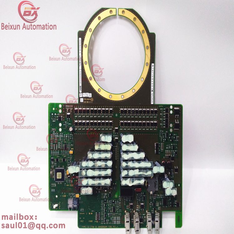
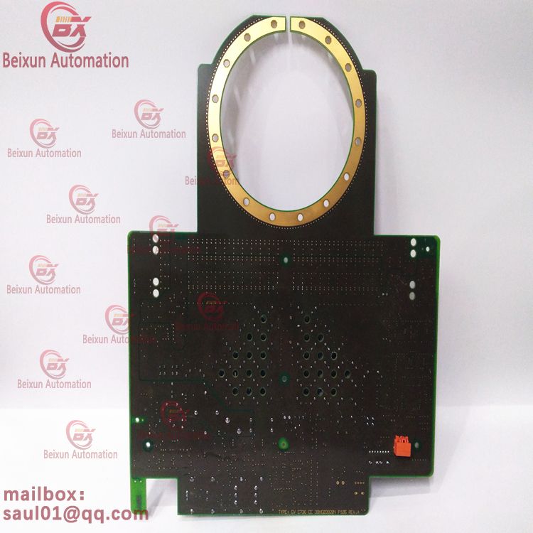
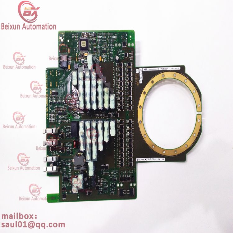
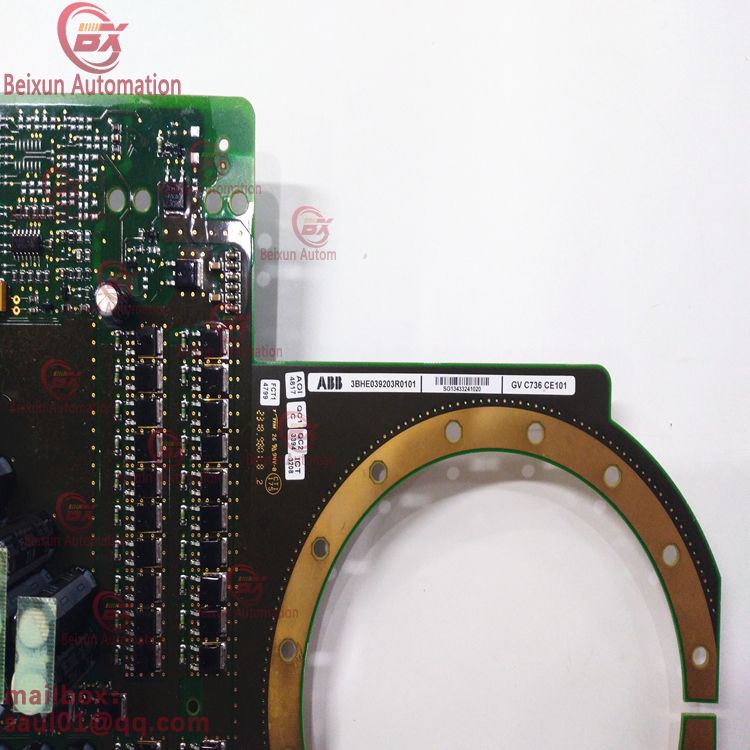
Abb 3bhe039203r0101 3bhe036204p201 3bhe039204p106 gvc736ce101

Abb 3bhe039203r0101 3bhe036204p201 3bhe039204p106 gvc736ce101

Abb 3bhe039203r0101 3bhe036204p201 3bhe039204p106 gvc736ce101

Abb 3bhe039203r0101 3bhe036204p201 3bhe039204p106 gvc736ce101

Abb 3bhe039203r0101 3bhe036204p201 3bhe039204p106 gvc736ce101